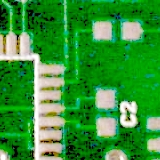
I’ve just finished my second and third printed circuit board designs and sent them off for production. The Spark Fun guys have a really cheap deal for hobbyists as long as you (1) aren’t in a huge hurry and (2) are willing to accept back what you send them. User beware, you have to proof you designs carefully as they aren’t going to do it for you. Which is why its cheap.
My first board was made for my small six-legged walking robot built by following the mechanical construction described in Karl Williams’ Insectronic book. In addition to the mechanics the book shows you how to make a circuit board using a PIC controller but I wanted to use an Atmel AVR. Plus I added an ultrasonic sensor with a pivoting head which required more pins than what the original design could support. Hence I made my own. It’s a very simple circuit (before laying out the board I built the whole thing on a breadboard in about 30 minutes). It uses an Atmel processor, a crystal oscillator, a bunch of headers and an LED or two. As I said, it’s simple. I really should find some time to take pictures + movies and post them, its a cool little robot.
This time I’m using surface mount packages for most everything on both boards. And these boards are more complicated. In addition to the Atmel processor, both are using a Microchip 2515 CAN controller + a transceiver. The first one is using a chip from FTDI that allows the processor to be accessible from USB. It’s basically going to be a bridge between my desktop or laptop and a CAN network. The second board doesn’t use the USB interface but instead plugs into a nifty little GPS module; this module requires a voltage level shifter to translate to the 2.85v used for serial communications rather than the 5v used by everything else. The idea is to create a board that reads GPS data and writes it back to the CAN network.
The last time I used the the Spark Fun service it worked out very well but I noticed the layout was shifted on the actual board a small amount from what I expected it to be. Fortunately I was very conservative with my traces so the board still works even if its not “perfect”. I used Eagle CAD again for these latest designs and carefully marked out the board size, thinking I must have made an error last time. But the Gerber files that got saved were offset again (and both boards were offset by a different amount). Seems like its a bug in Eagle.
I manually applied offsets and like magic the Gerbers lined up perfectly. The Spark Fun support forums talk about this issue but more about trying to fix it mechanically (and nobody else concludes its an Eagle bug so my conclusion might be hasty). My approach was to place “corner marks” at the four corners of the board directly onto the silk screen layer so it was included in the resulting Gerber files. Then I previewed the files in Pentalogix ViewMate and tweaked by hand until I could see the marks lining up correctly.
As soon as I get them back I’ll take some before and after assembly photos and post them.


 A few weeks ago I